Research Activities
1.Millimeter-wave and terahertz CMOS design
Millimeter-wave and its higher-frequency part “terahertz” have attracted many attentions to open up new applications such as ultrahigh-speed wireless communication and noninvasive transparent image. Utilizing recent transistor performance in CMOS technology, those new applications are being realized by commercial CMOS process. Since base-band signal processors are indispensable in a system level, CMOS circuits for millimeter-wave and terahertz have advantage against compound-semiconductor circuits from viewpoint of high-volume production and low-power consumption. In this talk, we will discuss millimeter-wave and terahertz CMOS design by clarifying difference from conventional microwave design. Design examples from system level to building block for mobile high-speed communication are also discussed.
2.Evaluation of ultrahigh-frequency CMOS devices
For realizing reproducible ultrahigh-frequency CMOS design, establishment of a dedicated process design kit (PDK) comprising layout library and its device model is essential. To achieve it, layout, measurement and parameter extraction are all important. In this talk, we will discuss how layout is performed and how subcircuit models for circuit simulation are extracted. We will also discuss how measurement will be done in ultrahigh-frequency band. In particular, several deembedding methods, which are important to obtain on-wafer characteristics, are compared and discussed.
3.CMOS injection-locked oscillators
Injection locked oscillators are versatile for realizing a frequency divider, a multiplier, clock synchronization, and so on. They are important technique to realize high-frequency, particularly millimeter-wave, synchronization using simple operation. In this talk, CMOS injection-locked oscillators are discussed from basic principle to measurement with referring to practical applications.
Research Policy
We create innovative designs that bring out the full performance of state-of-the-art LSI technology, to open up new possibilities for millimeter-wave broadband communication and terahertz security sensing. The key player in state-of-the-art electronics is the LSI. Up until now, the LSI has been responsible for dramatic improvements, which follow Moore's law that states the integration density quadruples every three years. However, improving the design technique of LSIs is indispensable for translating such improvement in integration into performance enhancement. We seek to achieve ultimate performance from the aspects of both ultrahigh frequency and low power by using creative designs of the state-of-the-art LSI. The evolution of design technology will contribute to both an expansion of the contents on the internet and an improvement in device portability. It is important to start our discussions from ground zero in order to achieve high performance in terms of both ultrahigh frequency and low power. In this approach, it is vital to regard nothing as taboo and not become a slave to convention. Empirical rules are not necessarily correct. Our current knowledge might not apply to reality. When boundary conditions change, common sense might become, in fact, nonsense. Our approach is to take common knowledge with a grain of salt, to discuss the applicability of a process for achieving our target, and to rectify illogical "common sense".
Message to Students
Each student will design, fabricate, and evaluate a state-of-the-art LSI utilizing world-class facilities. Varied and extensive knowledge on topics from semiconductor devices to social systems are important in our laboratory. Even if one's knowledge is limited, advanced knowledge can be obtained in a short time by interacting with laboratory members. Therefore, the key to advancing is to interact positively with each other in the laboratory. In our laboratory, students’ taking the initiative in discussions is very important.
Brief Bio
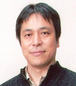
Minoru Fujishima received the B.E., M.E. and Ph.D degrees in Electronics Engineering from the University of Tokyo, Japan in 1988, 1990 and 1993, respectively. He joined faculty of the University of Tokyo in 1988 as a research associate, and was an associate professor of the School of Frontier Sciences, University of Tokyo since 1999. He was a visiting professor at the ESAT-MICAS laboratory, Katholieke, Universiteit Leuven, Belgium, from 1998 to 2000. Since 2009, he has been a professor of the Graduate School of Advanced Sciences of Matter, Hiroshima University.
He studied design and modeling of CMOS and BiCMOS circuits, nonlinear circuits, single-electron circuits, and quantum-computing circuits. His current research interests are in the designs of low-power millimeter- and short-millimeter-wave wireless CMOS circuits. He coauthored more than 40 journal papers and 100 conference papers, and a book entitled “Design and Modeling of Millimeter-Wave CMOS Circuits for Wireless Transceivers: Era of Sub-100nm Technology,” published by Springer, 2008.
He is a member of IEICE, IEEE, and JSAP. He is currently serving as a technical committee member of several international conferences.
 Millimeter-wave uncompressed HD transmission system |
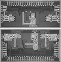
 Millimeter-wave CMOS circuits for uncompressed HD transmision |
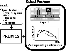
 PREMICS: design automation tool for millimeter/terahertz CMOS circuits |
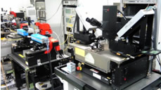
 On-wafer measurement system for millimeter-wave/terahertz CMOS devices |


